Page 18 - Spring Summer 2026
P. 18

Industry News                                                                                                                                                                                                    Industry News


                                                                                                                                                                                        The tellurium layers act as ‘highways’ in which mobile
                                                                                                                                                                                        electrons move rapidly and naturally forming repeating
                                                                                                                                                                                        wave-like patterns, whereas the cerium layers host
                                                                                                                                                                                        stationary electrons that remain localised and do not
                                                                                                                                                                                        move. The quantum property known as spin results in
                                                                                                                                                                                        these fixed electrons acting like bar magnets in a fixed
                                                                                                                                                                                        position.
                                                                                                                                                                                        The scientists used scanning tunnelling microscopy at


                                                                                                                                 quantum error correction. This validated individual
                                                                                                                                 qubits and two-qubit systems. Now, this has been
                                                                                                                                 extended to include the larger eight-qubit linear array
                                                                                                                                 whilst at the same time maintaining the coherence and
                                                                                                                                 control required for quantum operations.
          ADVANCES IN QUANTUM                                                                                                    It was also found that expanding the architecture for the
                                                                                                                                 larger array did not require a proportional increase in
          TECHNOLOGY                                                                                                             sensor numbers, wiring complexity or thermal load.

                                                                                                                                 Kristiaan De Greve comments:
                                                                                                                                                                                        temperatures close to absolute zero to map the surface
                                                                                                                                 “ The future of quantum computing depends not only
                                                                                                                                                                                        of the material at atomic resolution. It was observed
                                                                                                                                 on qubit quality, but also on the ability to manufacture
                                                                                                                                                                                        that the mobile electrons formed clear parallel stripes.
                                                                                                                                 increasingly complex quantum processors with the
                                                                                                                                                                                        A magnetic field was then applied which resulted in
                                                                                                                                 reproducibility, yield and scale of the semiconductor
                                                                                                                                                                                        ‘electronic frustration’ in which the electrons exhibited
                                                                                                                                 industry.
                                                                                                                                                                                        low-energy patterns without preferring any single one,
                                                                                                                                 This result demonstrates that industrial 300mm CMOS-   and reformed into a chequered pattern.
                                                                                                                                 compatible manufacturing can support quantum
          Quantum Dot Qubit fabricated with High NA                                                                                                                                     A companion study used neutron scattering to probe
                                                                                                                                 systems beyond isolated qubit pairs. By combining
          EUV Lithography                                                                                                        imec’s advanced semiconductor process technology       the material’s underlying magnetic core, and this
                                                                                                                                                                                        revealed that the material developed an unexpectedly
                                                                                                                                 with quantum device engineering, we taking important
          A first-of-its-kind quantum dot qubit device                                                                                                                                  complex magnetic order that directly supports and
                                                                                                                                 steps toward realising scalable silicon-based quantum
          produced using High Numerical Aperture extreme                                                                                                                                drives these shifting electronic states at near absolute
                                                                                                                                 processors. “
          ultraviolet lithography has been revealed by imec,                                                                                                                            zero.
          marking a turning point towards the industrial scale                                                                   Reference: Tyler, N., ‘Imec and Diraq demonstrate eight-qubit Silicon
          manufacture of quantum computing hardware.                                                                             Quantum Processor using CMOS Manufacturing’, New Electronics, 13th.   Yuita Fujisawa, co-first author of the study and assistant
                                                                                                                                                                                        professor at Hiroshima University, says:
                                                                                                                                 July
          Silicon quantum dot qubits rely on confining
                                                                                                                                                                                        “ CeTe3 offers a rare opportunity to watch mobile
          individual electrons in nanoscale silicon structures
          with the electron’s spin state used to represent                                                                       Japanese Scientists rewrite Rules inside               electrons and localised spins work together. We wanted
                                                                                                                                                                                        to directly visualise how this cooperation gives rise to
          quantum information. The fabrication process is                                                                        layered Quantum Material
                                                                                                                                                                                        collective electronic states.
          largely compatible with conventional CMOS chip
                                                                                                                                 Researchers at the Okinawa Institute of Science
          manufacturing, with High NA EUV lithography effectively                                                                                                                       We were astonished because it is extremely rare for a
                                                                                                                                 and Technology and Hiroshima University have
          shifting the focus from experimental demonstrations                                                                                                                           material to host multiple competing electronic patterns
                                                                                                                                 determined that a small magnetic nudge can be
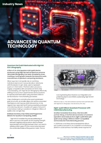
          to reproducible fabrication using standard 300mm         true engineering feat, thanks to our integration and                                                                 that can be switched so dramatically by such a small
          semiconductor manufacturing processes.                   patterning teams and ASML’s outstanding High NA EUV           used to transform a whole electronic landscape         magnetic field. “
                                                                                                                                 from parallel stripes to a neat chequerboard in a
                                                                   technology. “
          A key challenge is controlling the spacing between                                                                     layered sample of the quantum material cerium          Reference: Dixit, M., ‘Quantum Material’s Electronic States can be
          gate structures, as smaller gaps can reduce unwanted   Reference: Tyler, N., ‘imec demonstrates Quantum Dot Qubit fabricated   tritelluride (CeTe3), potentially illustrating how future   flipped with Magnetic Field, Study finds’, Interesting Engineering, 23rd.
          interference and improve qubit interactions. In this   with High NA EUV Lithography’, New Electronics, 19th. May       spintronics and quantum computing architectures        July
          regard imec reported that it had successfully produced                                                                 may control information at the atomic scale.
          a functioning network  of qubits with gaps of around 6
                                                                Eight-qubit Silicon Quantum Processor with                       In materials such as copper, silver and silicon, electrons   New Benchmark for Quantum safe
          nanometres, making it possible to integrate millions of
                                                                CMOS Manufacturing                                               behave in predictable ways. By comparison, in          Transatlantic Data Transmission
          qubits onto a single chip.
                                                                                                                                 quantum materials complex interactions give rise to
                                                                Another innovation from imec, this time with                                                                            Colt Technology Services and Ciena have completed
          Kristiaan De Greve, imec Fellow and Programme                                                                          collective electronic states. Consequently there is a
                                                                partner Diraq, is the first demonstration of coherent                                                                   one of the fastest quantum safe data transmissions
          Director for Quantum Computing, states:                                                                                goal in quantum materials research to understand how
                                                                operation and readout of an eight-qubit MOS spin-                                                                       ever demonstrated and the fastest across a
            “ High NA EUV enables the precise patterning of     qubit array using a 300mm CMOS-compatible                        these emergent states develop so that they can be      transatlantic route. Live data running was protected
            silicon quantum dot qubits. As the coupling strength   semiconductor manufacturing process.                          manipulated and controlled.                            over 6,900km of Colt’s subsea and terrestrial
            between neighbouring quantum dots increases                                                                          CeTe3 is similar to graphene in that it is a two-      network between New York and London with Ciena’s
                                                                In 2025 imec and Diraq demonstrated that silicon
            exponentially with the gap between them, we need to                                                                  dimensional layered material with ultrafast mobile     WaveLogic 6 Extreme (WL6e) encryption.
                                                                spin qubits produced on an industrial manufacturing
            reliably pattern gaps of a few nanometres between                                                                    electrons. Unlike graphene, however, CeTe3 contains
                                                                platform could achieve the fidelity levels required for
            the control electrodes of the quantum dots. This is a                                                                two types of atoms, namely tellurium and cerium.
             18                                                                                                                                                                                                                   19
                                                                            Become a member: https://membermojo.co.uk/ie         Become a member: https://membermojo.co.uk/ie
                                                                    Become a subscriber: https://membermojo.co.uk/subscriber     Become a subscriber: https://membermojo.co.uk/subscriber
                                                                        Become a sponsor: https://membermojo.co.uk/sponsor       Become a sponsor: https://membermojo.co.uk/sponsor
   13   14   15   16   17   18   19   20   21   22   23