


Page 25 - Autumn 2024
P. 25
manipulate the properties of light and can be used
                                                                to produce holograms. They have applications in
                                                                areas such as data storage, optical displays and
                                                                high numerical aperture lenses such as those used in
                                                                optical microscopy and sensing.
                                                                The researchers found that when each meta-atom
                                                                is carefully shaped to control the properties of the
          The technology incorporates a proprietary closed-     beam of light that passes through it, it behaves as
          loop digital stabilisation system that actively       a pixel of the HM. When light passes through the HM,
          compensates for thermal drift, ensuring continuous,   at each pixel, the properties of the light become
          low-error transmission over wide temperature          slightly modified. This makes it possible to create a
          fluctuations. Architectural innovations make the      pre-designed image on the other side, utilising the
          Passage 3D CPO platform inherently polarisation       principle of interference through which light waves
          insensitive, ensuring robust performance even         create complex patterns when they interact.
          when the fibres are being handled or subject to
                                                                So far scientists have only been able to make very
          mechanical stress.
                                                                simple shapes with OLEDs, limiting their usability, but
          The combination of fibre bandwidth density, efficient   with this advance miniaturised and highly integrated
          spectral utilisation and robust performance are       metasurface displays become possible.
          seen as making Lightmatter’s Passage technology
          foundational to the transition from electrical to
          optical interconnects in AI data centres.
          Nicholas Harris, Founder and CEO of Lightmatter,
          states:

            “Data centres are the new unit of compute in the AI
            era, with the next 1000x performance gain coming
            largely from ultra-fast photonic interconnects. One
            16-lambda bidirectional link is an architectural leap
            forward. Hyperscalers can achieve significantly
            higher bandwidth density with standard single-
            mode fibre, reducing both capital expenditure
            and operational complexity, while enabling higher
            ‘radix’ - more connections per XPU or switch”.
          Reference: Tyler, N., New Electronics, 19th. August


          Holograms set to transform Smart Devices
          Researchers from the School of Physics and
          Astronomy at the University of St. Andrews have
          created a new optoelectronic device from the
                                                                Andrea Di Falco, Professor of Nano-photonics at the
          combined use of Holographic Metasurfaces
                                                                School of Physics and Astronomy, states:
          (HMs) and Organic Light Emitting Diodes (OLEDs)
          with the potential to transform smart devices,           “Holographic metasurfaces are one of the most
          communications, gaming and entertainment.                versatile material platforms to control light.
                                                                   With this work we have removed one of the
          Until now, holograms have been created using lasers,     technological barriers that prevents the adoption
          but at St. Andrews researchers have found that OLEDs     of metamaterials in everyday applications. This
          and HMs are able to provide a simpler and more           breakthrough will enable a step change in the
          compact method that is potentially both cheaper          architecture of holographic displays for emerging
          and easier to apply, enabling hologram technology        applications, for example in virtual and augmented
          to be much more widely deployed.                         reality”.

          OLEDs are thin film devices that are widely used to   Professor Graham Turnbull, also of the School of
          produce the coloured pixels in mobile phone displays   Physics and Astronomy, adds:
          and some televisions. They are a flat, surface-
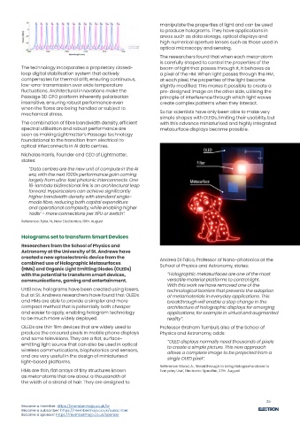
                                                                   “OLED displays normally need thousands of pixels
          emitting light source that can also be used in optical
                                                                   to create a simple picture. This new approach
          wireless communications, biophotonics and sensors,
                                                                   allows a complete image to be projected from a
          and are very useful in the design of miniaturised
                                                                   single OLED pixel”.
          light-based platforms.
                                                                Reference: Wood, A., ‘Breakthrough to bring Holograms closer to
          HMs are thin, flat arrays of tiny structures known    Everyday Use’, Electronic Specifier, 27th. August
          as meta-atoms that are about a thousandth of
          the width of a strand of hair. They are designed to

                                                                                                           25
          Become a member: https://membermojo.co.uk/ie
          Become a subscriber: https://membermojo.co.uk/subscriber
          Become a sponsor: https://membermojo.co.uk/sponsor

